From Electronics I Laboratory Manual
A common-emitter amplifier1 in general will include three coupling capacitors that play an important role in the low-frequency response of the system. These capacitors are the input and output coupling capacitors2 and the emitter biapass capacitor3.
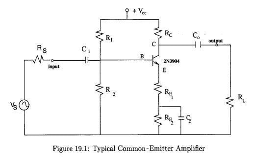 Figure 19.1 shows a typical common-emitter amplifier with a source, Vs (including its source resistance, Rs) and a load, RL. The low-frequency response of this amplifier is determined in part by these three capacitors (Ci, Co and CE). The result is essentially a combination of three high-pass filter networks that allow signals having frequencies greater than the cutoff frequency of the dominant network to pass through while attenuating all others. This frequency is the so-called 3-dB point. At this frequency, as you should know, the voltage is only 70.7% of the mid-frequency gain, or in decibels, it is the frequency at which the gain is 3-dB below the mid-frequency gain.
Each one of the three capacitors makes a contribution to the overall frequency response of the amplifier. Each one behaves like the capacitor in a high–pass filter. Therefore, each one will contribute with a cutoff frequency of its own. The cutoff frequencies for each capacitor are given by the following equations:
Each one of the three capacitors makes a contribution to the overall frequency response of the amplifier. Each one behaves like the capacitor in a high–pass filter. Therefore, each one will contribute with a cutoff frequency of its own. The cutoff frequencies for each capacitor are given by the following equations:
fci The cutoff frequency due to the input coupling capacitor, Ci, is given by
fCo The critical frequency due to the output coupling capacitor, Co, is given by
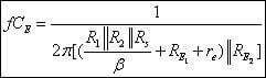
fcE Finally, the cutoff frequency due to the emitter bypass capacitor, CE, is
For the common-emitter amplifier shown in Fig. 19.1 the voltage gain is given by
where
and IE is the quiescent dc emitter current.
The voltage gain in decibels is given by the following equation
(19.1) |
(19.2) |
 | (19.3) |
|
(19.4) | ||
 |
 | (19.5) |
The voltage gain in decibels is given by the following equation
| (19.6) |
1 Or basically any other type of amplifier.
2 They are important if you want to keep the input and output voltages as pure ac voltages.
3 This is important to produce a high voltage gain.
Source: http://www.globalspec.com/reference/9649/359749/Amplifier-Low-Frequency-Response
Source: http://www.globalspec.com/reference/9649/359749/Amplifier-Low-Frequency-Response
No hay comentarios:
Publicar un comentario