domingo, 21 de marzo de 2010

Frequency compensation


In electrical engineering, frequency compensation is a technique used in amplifiers, and especially in amplifiers employing negative feedback. It usually has two primary goals: To avoid the unintentional creation of positive feedback, which will cause the amplifier to oscillate, and to control overshoot and ringing in the amplifier's step response.

Explanation

Most amplifiers use negative feedback to trade gain for other desirable properties, such as decreased distortion or improved noise reduction. Ideally, the phase characteristic of an amplifier's frequency response would be constant; however, device limitations make this goal physically unattainable. More particularly, capacitances within the amplifier's gain stages cause the output signal to lag behind the input signal by 90° for each pole they create.[1] If the sum of these phase lags reaches 360°, the output signal will be in phase with the input signal. Feeding back any portion of this output signal to the input when the gain of the amplifier is sufficient will cause the amplifier to oscillate. This is because the feedback signal will reinforce the input signal. That is, the feedback is then positive rather than negative.
Frequency compensation is implemented to avoid this result.
Another goal of frequency compensation is to control the step response of an amplifier circuit as shown in Figure 1. For example, if a step in voltage is input to a voltage amplifier, ideally a step in output voltage would occur. However, the output is not ideal because of the frequency response of the amplifier, and ringing occurs. Several figures of merit to describe the adequacy of step response are in common use. One is the rise time of the output, which ideally would be short. A second is the time for the output to lock into its final value, which again should be short. The success in reaching this lock-in at final value is described by overshoot (how far the response exceeds final value) and settling time (how long the output swings back and forth about its final value). These various measures of the step response usually conflict with one another, requiring optimization methods.
Frequency compensation is implemented to optimize step response, one method being pole splitting.


Use in operational amplifiers

Because operational amplifiers are so ubiquitous and are designed to be used with feedback, the following discussion will be limited to frequency compensation of these devices.
It should be expected that the outputs of even the simplest operational amplifiers will have at least two poles. An unfortunate consequence of this is that at some critical frequency, the phase of the amplifier's output = -180° compared to the phase of its input signal. The amplifier will oscillate if it has a gain of one or more at this critical frequency. This is because (a) the feedback is implemented through the use of an inverting input that adds an additional -180° to the output phase making the total phase shift -360° and (b) the gain is sufficient to induce oscillation.
A more precise statement of this is the following: An operational amplifier will oscillate at the frequency at which its open loop gain equals its closed loop gain if, at that frequency,
1. The open loop gain of the amplifier is ≥ 1 and
2. The difference between the phase of the open loop signal and phase response of the network creating the closed loop output = -180°. Mathematically,
ΦOL – ΦCLnet = -180°
Practice
Frequency compensation is implemented by modifying the gain and phase characteristics of the amplifier's open loop output or of its feedback network, or both, in such a way as to avoid the conditions leading to oscillation. This is usually done by the internal or external use of resistance-capacitance networks.
[edit]Dominant-pole compensation
The method most commonly used is called dominant-pole compensation, which is a form of lag compensation. A pole placed at an appropriate low frequency in the open-loop response reduces the gain of the amplifier to one (0 dB) for a frequency at or just below the location of the next highest frequency pole. The lowest frequency pole is called the dominant pole because it dominates the effect of all of the higher frequency poles. The result is that the difference between the open loop output phase and the phase response of a feedback network having no reactive elements never falls below −180° while the amplifier has a gain of one or more, ensuring stability.
Dominant-pole compensation can be implemented for general purpose operational amplifiers by adding an integrating capacitance to the stage that provides the bulk of the amplifier's gain. This capacitor creates a pole that is set at a frequency low enough to reduce the gain to one (0 dB) at or just below the frequency where the pole next highest in frequency is located. The result is a phase margin of ≈ 45°, depending on the proximity of still higher poles.[2] This margin is sufficient to prevent oscillation in the most commonly used feedback configurations. In addition, dominant-pole compensation allows control of overshoot and ringing in the amplifier step response, which can be a more demanding requirement than the simple need for stability.
Though simple and effective, this kind of conservative dominant pole compensation has two drawbacks:
1. It reduces the bandwidth of the amplifier, thereby reducing available open loop gain at higher frequencies. This, in turn, reduces the amount of feedback available for distortion correction, etc. at higher frequencies.
2. It reduces the amplifier's slew rate. This reduction results from the time it takes the finite current driving the compensated stage to charge the compensating capacitor. The result is the inability of the amplifier to reproduce high amplitude, rapidly changing signals accurately.

Often, the implementation of dominant-pole compensation results in the phenomenon of Pole splitting. This results in the lowest frequency pole of the uncompensated amplifier "moving" to an even lower frequency to become the dominant pole, and the higher-frequency pole of the uncompensated amplifier "moving" to a higher frequency.
Other methods
Some other compensation methods are: lead compensation, lead–lag compensation and feed-forward compensation.
Lead compensation. Whereas dominant pole compensation places or moves poles in the open loop response, lead compensation places a zero[3] in the open loop response to cancel one of the existing poles.
Lead–lag compensation places both a zero and a pole in the open loop response, with the pole usually being at an open loop gain of less than one.
Feed-forward compensation uses a capacitor to bypass a stage in the amplifier at high frequencies, thereby eliminating the pole that stage creates.
The purpose of these three methods is to allow greater open loop bandwidth while still maintaining amplifier closed loop stability. They are often used to compensate high gain, wide bandwidth amplifiers.

The Dominant Pole approximation

Reduction of a second order system to first order

Consider a second order system with a transfer function that is reduced to first order.


This assumes that a>>b, or that the pole at b is dominant. The coefficient "a" remains in the denominator so that the DC gain (which is also the final value of the output with a unit step input) remains unchanged. Recall that the DC gain is G(0).

The graph below shows the exact response (red) and the dominant pole approximation (green) for a=8 and b=1. Following the graph is Matlab code in which you can set a with b=1 to see how accurate the dominant pole approximation is.

Example


Higher Order

The dominant pole approximation can also be applied to higher order systems. Here we consider a third order system with one real root, and a pair of complex conjugate roots.


In this case the test for the dominant pole compare "a" against "zwn". This is because "zwn" is the real part of the complex conjugate root (we only compare the real parts of the roots when determining dominance because it is the real part that determines how fast the response decreases). Note that the DC gain of the exact system and the two approximate systems are equal.

In the examples and Matlab code below, the second order pole has zeta=0.4 and wn=1 (which yields roots with a real part of 0.4 and an imaginary part of +/-0.92j). There are three graphs. In the first graph a=0.1 (the real pole dominates), in the second graph a=4 (the complex conjugate poles dominate) and in the third graph a=0.4 (neither dominates and the response is obviously more complicated than a simple second order response). In all three graphs the exact response is in red, the approximate response in which the first order pole dominates is in green, and the approximate response in which the second order pole dominates is in blue.

Examples:


Invite your mail contacts to join your friends list with Windows Live Spaces. It's easy! Try it!

Understanding Speaker Frequency Response


The Secret Behind The Industry's Most-Cited Spec.
Here's a quick quiz: which of these two speakers sounds better: Speaker A with a frequency response range of 45Hz to 18kHz or, Speaker B with a range of 20Hz to 25kHz? The truth is there's simply not enough data in these numbers to know anything of value. Taken out of context and without other data, a simple set of numbers don't tell you much about real world sound quality. But people make audio buying decisions based on published specifications, such as the frequency response spec, everyday. I'd like to demystify the process for you; let you in on a little industry secret about "The Frequency Response Spec."

My Frequency Response
The Frequency Response specification attempts to describe the range of frequencies or musical tones a speaker can reproduce, measured in Hertz (known to old-timers as "Cycles per Second"). The range of human hearing is generally regarded as being from 20Hz, very low bass tones, through 20kHz (20,000Hz), the very highest treble. Presumably a speaker that could reproduce that range would sound lifelike. Alas, it is no guarantee. The most important determinant of a speaker's frequency performance is not its width or range, but whether it's capable of reproducing all the audible frequencies at the same volume at which they were recorded.

You don't want the speaker to change the "mix" of tones; that would ruin the timbre of voices and instruments, making them sound unnatural. Ideally, you want the sounds that are on the recording to be reproduced as they were recorded, without the speaker changing the sound. To say it another way: if you made a recording of all the audible tones at the same volume and played that recording through a speaker, you'd want all the audible tones to come out at the same volume. In fact, that's one way of measuring speakers. A signal that's comprised of all frequencies at equal volume is fed into a speaker that sits in a room with no reflective surfaces. A calibrated microphone is placed in front of the speaker and feeds the speaker's output into a machine that plots the frequency vs. amplitude as shown in Figure A.


Now take a look at the graph in Figure B. That's the frequency response of the Erehwon Model 10, with drivers and tweeters made of pure Unobtainium ("Half the carbs, all the sound!"). The flat line on the graph indicates that the speaker is "flat"; it reproduces all the musically relevant tones at the same volume. That doesn't mean that a "flat" speaker will play all recorded sounds at the same volume -- bear with me here -- it means that it will treat all sounds equally; it won't impose its will on the music but will allow you to hear the music as it was recorded. Flat is good. Flat response means that the speaker reproduces sound accurately.


Too bad that the Erehwon Model 10 doesn't really exist, and neither does Unobtainium. Today's technologies allow speaker designers to get closer to the "flat" ideal than ever before, but they still fall far short of "perfection." So if a frequency range spec is not adequate, what is?

Frequency Response In Context
A big improvement would be a frequency response number that also includes the amplitude tolerance, expressed as "XHz-YkHz +/- 3dB." This tells you that the amplitude of the speaker's response relative to frequency does not deviate more than 3 Decibels from the center line. The "plus or minus 3dB" spec is regarded as a standard of sorts. The theory is that 3dB differences are "just perceptible," so a speaker whose response curve lies within that tolerance window is a reasonably accurate speaker. Let's see if that idea holds water.


Take a look at Figure C. This speaker has response that can be specified as 20Hz-20kHz +/- 3dB. Take a look at Figure D; it, too, can have the exact same specification as Speaker C! Do you think they will sound similar? NOT! They won't sound even remotely like one another. Speaker C will have "one note" bass and will make voices and other instruments sound unnatural, but Speaker D will sound smooth and more natural.


If I had to choose strictly by the response curves, I'd choose speaker D because its amplitude variations are smoother and gentler. In contrast, speaker C's amplitude variations are more extreme and "spikey." Experience has shown speaker designers that those rapid changes in response produce a sound that is more fatiguing, less pleasing and subjectively less accurate.


Now look at the response of the speaker in Figure E. This speaker exhibits a smooth response curve with low amplitude variations so you'd expect a fairly natural sound; however, the bandwidth of these errors is very broad, and experience has shown us that even low volume variations are audible if they cover a broad range of frequencies. In this case, Speaker E would have rich bass, prominent treble and be somewhat recessed or "laid back" in the midrange. Audiophiles call this "The Smile Curve." It's not the desirable trait it sounds like but it's a very "sellable" trait to naïve buyers.

My Response To Frequency
Now that you know the importance (and limitations) of amplitude variations in frequency response graphs, you might ask: "does the frequency range tell us anything at all?" Yes, it does. As long as you know the amplitude tolerance (+/- 3dB), the frequency response range or width tells you how high or low the speaker goes. A speaker rated as 20Hz - 25kHz +/- 3dB will play lower bass and higher treble sounds than a speaker that measures 40Hz - 20kHz +/- 3dB. I wouldn't bet money that it would be the better, more enjoyable speaker, but at least I'd know something of value.

And now that you know how to interpret these numbers, you're ready to run right out and buy a speaker just by looking at the response curve, right? I wouldn't recommend it. Despite many advances in technology over the past 20 years, frequency response measurement is an imperfect science. The same speaker measured by two different labs may yield different response graphs. And some companies just plain cheat when they publish response curves. If it looks hand drawn, it probably was. ( Yes, the graphs were hand drawn for illustration purposes.)

The Third Dimension
So far we've talked about frequency (the X axis of the graph) and amplitude (Y axis) but we left out an important third dimension: time. When a speaker responds to an impulse, for example a rim shot -- "THWACK!" -- it should start instantly and stop the instant the instrument stops making sound. If the speaker keeps vibrating or resonating and making sound after the source sound stops it's changing, or "coloring," the sound of the original recording. And that's bad.


Figure F shows a bandwidth limited impulse signal. You can see that it starts and stops abruptly. Figure G shows that same impulse coming out of a speaker. You can see that the sound persists after the impulse input has stopped -- it resonates or "rings." The speaker is changing the timbre or character of the original recording. In order to see to what extent and at which frequencies the "ringing" is happening, we use a sophisticated computer algorithm called MLLSA (affectionately called "Melissa" by engineers who don't date much) to measure the response of a speaker in frequency, amplitude and time. Figure H is a MLLSA spectral decay graph of a prototype speaker. The third axis of this graph is time, so graph lines closest to you are measurements taken later than the ones in the back. Think of it as a series of slices with each slice being a frequency response graph taken at a different point in time.

If we were to measure the perfect speaker the MLLSA graph would look like a straight line in back with no lines in front. Real speakers fall far short of this ideal and continue to resonate after an impulse has stopped, such as in Figure H. Figure I is a Polk LSi9, and we can see that the speaker stops responding sooner in the midrange than the speaker pictured in Figure H, indicating that the LSi9 is a better sounding speaker.


While no measurement technique can fully describe the subjective sound of a louds peaker, MLLSA and other frequency response measurements are of great help to Polk engineers in developing better sounding speakers. Only a fool would design a speaker based on measurements alone and only a total fool would design a speaker based solely on subjective listening. A speaker that might sound good on a particular recording may in fact be flawed - it may have what is commonly called a "euphonic coloration." It may be pleasing to the ear under certain conditions, but it sure ain't right.

We use both measurements and subjective listening to design and evaluate speakers. The measurements save us time and are a great help in pointing us in the right design direction, avoiding mistakes that may come back to bite us later. The measurements give us a means of selecting which experimental designs are worth listening to. But we have to be satisfied with the total subjective experience before a new design becomes a Polk Audio speaker. We spend countless hours listening to music and movies. Several experienced listeners have to listen to a proposed design and sign off on the sound before a model can even go into production. The Project Manager, Systems Engineer, VP of Engineering, Product Line Manager, and especially Matthew Polk, all have to agree that the prototype delivers the kind of rewarding listening experience that you expect from Polk Audio.

What's Your Frequency?
You now know the secret: a frequency response specification is a very weak predictor of the actual performance of a loudspeaker. A frequency response chart can be more helpful, but it's missing the important time measurement. You now know to look for overall curve smoothness and to avoid rapid swings in amplitude. Some magazines and review sites publish MLSSA graphs of reviewed speakers, and now you'll understand how to interpret them. More power to you!

No matter how adept you might be at interpreting frequency response data, it should only be one data point among many in choosing a speaker. There is so much more to a speaker's performance than just its response - like its dispersion and imaging, dynamic range and detail resolution as well as size, cosmetics and price. Looking at good frequency response data can help you eliminate speakers with obvious and obnoxious errors. Once you've eliminated the boom & tizz pseudo-fi speakers, you can settle down to careful listening and making a more informed choice.

How Polk Specifies Frequency Response
Polk Audio publishes two frequency response specifications: "Overall" and "-3dB." "Overall" describes the frequency range limits of the speaker within an amplitude drop off of 9dB. Any frequency re p roduced more than 9dB down from the rest of the frequencies will contribute little to the sound. The "-3dB" spec describes the frequency range limits of the speaker within an amplitude drop off of 3dB.

I just wrote this big article making the case that these kinds of numbers are not terribly useful in making buying decisions. So why does Polk use them? For better or for worse, these numbers are the norm in the audio industry. To not publish them would leave an impression that our products were not competitive. A better question would be: why don't we publish frequency response and MLSSA graphs in addition to the simple numbers? We feel that these graphs would not be meaningful to the vast majority of consumers. It takes years of working with measurements and loudspeakers before you get a good sense of how the graphs correlate to subjective sound quality. Incorrect interpretation of graphs can easily lead to misinformation and bad choices. Finally, the variation in measurement techniques can make comparing graphs from two different labs or manufacturers unreliable and misleading.

Lenny Z Perez M
EES


Invite your mail contacts to join your friends list with Windows Live Spaces. It's easy! Try it!

Basic Circuits - Bypass Capacitors


The Function

The definition of a bypass capacitor can be found in the dictionary of electronics.

Bypass capacitor: A capacitor employed to conduct an alternating current around a component or group of components. Often the AC is removed from an AC/DC mixture, the DC being free to pass through the bypassed component.
In practice, most digital circuits such as microcontroller circuits are designed as direct current (DC) circuits. It turns out that variations in the voltages of these circuits can cause problems. If the voltages swing too much, the circuit may operate incorrectly. For most practical purposes, a voltage that fluctuates is considered an AC component. The function of the bypass capacitor is to dampen the AC, or the noise. Another term used for the bypass capacitor is a filter cap.


n the chart on the left, you can see the what happens to a noisy voltage when a by-pass capacitor is installed. Notice that the differences in voltage are pretty small (between 5 and 10 millivolts). This graph represents a small range of 4.95 volts to 5.05 volts. Random electrical noise causes the voltage to fluctuate, as you can see in graph. This is often called 'noise' or 'ripple'. The blue line, represents the voltage of a circuit that doesn't have a bypass. The pink line is a circuit that has a bypass. Ripple voltages are present in almost any DC circuit. You can see even with the bypass, the voltage does fluctuate, even though it is to a smaller degree. The key function of the bypass capacitor is to reduce the amount of ripple in a circuit. Too much ripple is bad, and can lead to failure of the circuit. Ripple is often random, but sometimes other components in the circuit can cause this noise to occur. For example, a relay or motor switching can often times cause a sudden fluctuation in the voltage. Much like disturbing the water level in a pond. The more current the other component uses, the bigger the ripple effect.

A fair question to ask is why does this small fluctuation matter? Gee, isn't the voltage close enough? The answer depends on the type of circuit you are designing. If you are just running a motor connected to a battery, or perhaps an LED, then chances are the ripple doesn't matter much to you. However, if you are using digital logic gates, things get slightly more complex, and this ripple can cause problems in the circuit.

Lets consider for just a moment what the effect of the ripple voltage is. Basic electrical theory tells us that a voltage is a difference in potential. It tells us that a current will flow across this difference in potential. We know that the larger the voltage, the larger the current. We also know the direction of the voltage determines the direction of the current.

Consider the graphs on the right. The top graph shows a pair of ripple voltages that I enlarged to make them easier to see. Just like the previous graph, the blue line represents the circuit without the bypass cap, and the other line is with the bypass cap. By looking along the bottom axis of the graph, you can see that starting at point 2 that the voltage is increasing. By looking in the Ripple Current chart, point 2 shows that the current is a relatively large magnitude in one direction. In contrast, point 5 shows the voltage and current going the other direction.
Notice the difference between the values with and without the bypass cap. By dampening the ripple voltage, the bypass cap also dampens the ripple current. I would like to point out that the Ripple Voltage chart and the Ripple Current charts clearly show an alternating current. You can see how the voltage swings, and how the current changes directions. Even though this is is a DC circuit, the ripple is causing an AC component. The bypass capacitor is helping to reduce this AC component.

The ripple current acts like an eddie or backflow in the circuit. As the fluctuating voltages and currents propogate through the circuit, differences in voltages and currents can occur that cause the circuit to fail. For example, assume that a AND gate is holding its state because the semiconductors that make up the gate are in a stable state. Transistors work by currents flowing one direction through the gate. If the current stops flowing, the transistor shuts down. If a ripple current comes through where the current momentarily flows the wrong direction, the gate will shutdown, and you will see a change it its output. This can cause a cascading failure, because one gate may be connected to many other gates.


To summarize, the bypass capacitor is used to dampen the AC component of your DC circuits. By installing bypass capacitors, your DC circuit will not be as susceptable to ripple currents and voltages.

Using Bypass capacitors


Many schematics that you find published in magazines and books leave the bypass capacitors out. They assume you know to put them in. Other times you will find a little row of capacitors (caps) stuck off in the corner of the schematic with no apparent function. These are usually the bypass (or filter) caps. If you pickup almost any digital circuit, you will find a bypass capacitor on it.


The most simple incarnation of the bypass capacitor is a cap connected directly to the power source and to ground, as shown in the diagram to the left. This simple connection will allow the AC component of VCC to pass through to ground. The cap acts like a reserve of current. The charged capacitor helps to fill in any 'dips' in the voltage VCC by releasing its charge when the voltage drops. The size of the capacitor determines how big of a 'dip' it can fill. The larger the capacitor, the larger the 'dip' it can handle. A common size to use is a .1uF capacitor. You will also see .01uF as a common value. The precise value of a bypass cap isn't very important.

So, how many bypass capacitors do you really need? A good rule of thumb I like to use is each IC on my board gets its own bypass capacitor. In fact, I try to place the bypass cap so it is directly connected to the Vcc and Gnd pins. This is probably overkill, but it has always served me well in the past, so I will recommend it to you. It turns out you can even by DIP sockets that have the bypass caps built in. I suppose once you reach more than a few capacitors per square inch, you might be able to let up a bit!

Another great place for a bypass cap is on power connectors. Anytime you have a power line heading off to another board or long wire, I would recommend putting in a bypass cap. Any long length of wire is going to act like a little antenna. It will pick up electrical noise from any magnetic field. I always put a bypass cap on both ends of such lengths of wire.

The frequency of the ripple can have a role in choosing the capacitor value. Rule of thumb is the higher the frequency, the smaller the bypass capacitor you need. If you have very high frequency components in your circuit, you might consider a pair of capacitors in parallel. One with a large value, one with a small value. If you have very complex ripple, you may need to add several bypass capacitors. Each cap is targeting a slightly different frequency. You may even need to add a larger electrolytic cap in case the amplitude of the lower frequencys is too great. For example, the circuit on the right is using three different capacitor values in parallel. Each will respond better to different frequencies. The 4.7uF cap (C4) is used to catch larger voltage dips which are at relatively low frequencies. The cap C2 should be able to handle the midrange frequencies, and C3 will handle the higher frequencies. The frequency response of the capacitors is determined by their internal resistance and inductance.

Summary

Bypass capacitors help filter the electrical noise out of your circuits. They do this by removing the alternating currents caused by ripple voltage. Most digital circuits have at least a couple of bypass capacitors. A good rule of thumb is to add one bypass capacitor for every integrated circuit on your board. A good default value for a bypass cap is 0.1uF. Higher frequencies require lower valued capacitors.

Lenny Z Perez M
EES


Connect to the next generation of MSN Messenger  Get it now!

The Miller’s theorem


The Miller's theorem establishes that in a linear circuit, if there exists a branch with impedance Z, connecting two nodes with nodal voltages V1and V2, we can replace this branch by two branches connecting the corresponding nodes to ground by impedances respectively Z / (1-K) and KZ / (K-1), where K = V2 / V1.


In fact, if we use the equivalent two-port network technique to replace the two-port represented on the right to its equivalent, it results successively:


And, according to the source absorption theorem, we get the following:


As all the linear circuit theorems, the Miller's theorem also has a dual form:

Miller's dual theorem

If there is a branch in a circuit with impedance Z connecting a node, where two currents I1 and I2 converge, to ground, we can replace this branch by two conducting the referred currents, with impedances respectively equal to (1+ a) Z and (1+ a) Z / a, where a = I2 / I1.


In fact, replacing the two-port networkby its equivalent, as in the figure,


it results the circuit on the left in the next figure and then, applying the source absorption theorem, the circuit on the right.


Miller's theorem applies to the process of creating equivalent circuits. This general circuit
theorem is particularly useful in the high-frequency analysis of certain transistor amplifiers at
high frequencies.


The Miller Theorem (and "Effect")

Suppose that we have two networks separated by a bridging element Y. The equivalent circuits shown above represent particular important examples of such a situation


Further, suppose that we can establish the following "gain relationship" by independent means:


and, thus, we may write


If everything else remains unchanged, this bridged configuration can be replaced by a configuration of "decoupled" networks as follows:


where by equivalence we must have


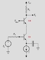
The Classic Solution to the "Miller Effect"
The Cascode Amplifier


Lenny Z Perez M
EES


Explore the seven wonders of the world Learn more!

Square Wave Testing.


It is perhaps unfortunate that the most common test for stability is to look for 'ringing' on a square-wave test signal. It is instructive to look at some examples, here using a 2kHz square wave input.


The first looks like sustained low level oscillation around 30kHz, while the second looks like damped oscillation at the same frequency. Actually the first diagram has nothing at all added to the square wave, the only thing done was to remove everything above the 15th harmonic. Everything up to and including 30kHz is being reproduced with no distortion, no phase error and flat frequency response. (If possible see 'A check on Fourier' by M.G.Scroggie, Wireless World, Nov 1977. p79-82. His Fig.5 is a better drawn version showing the harmonics and how they add.) The lack of higher frequency components however gives the impression of a serious problem, when in fact the audio frequency reproduction is perfect, and there is nothing at all added or removed in this range. The symmetrical variation of the 'oscillation' amplitude gives a clue to the origin of the effect, but practical low pass filters give a less sharp cut off of high harmonics together with frequency dependant phase shift which will give a different appearance. The suggestion that 'ringing' needs to be minimised is not entirely convincing when even an ideal low-pass filter gives the above result. Using an audio signal with no frequency components above 30kHz instead of the square wave there would be no effect at all from this filter.
The second diagram can also be the result of low-pass filtering, and something similar is often produced by the interaction of output inductors with capacitive loads, which is not related in any direct way to stability. Checking the signal ahead of the inductor may reveal a smooth signal without the 'ringing' effect, though some amplifiers have an output impedance with a small internal inductive component which will add some small effect. The square-wave response shown in the MJR-6 test results shows low level 'ringing' which is estimated at 120kHz. This is close to the expected resonance frequency of the 0.4uH output inductor with the 4uF load capacitance used in that test. Increasing loop gain to the point where the amplifier becomes unstable caused oscillation around 6MHz, as expected from the feedback loop unity gain frequency. This demonstrates that output 'ringing' is generally not related to instability, which can occur in an entirely different frequency range, and unless the input signal includes components close to the LC resonance frequency, or the inductance used is too high, there will be little effect. Leaving out the output inductor to eliminate 'ringing' caused by this LC resonance may seriously reduce the phase margin at higher frequencies with some capacitive loads, dangerously increasing the risk of instability.
A square wave test to investigate stability into capacitive loads is therefore of limited usefulness, and may be seriously misleading. My experience is that amplifiers sometimes have a stable state and an unstable state, and triggering them into instability may need a precise choice of load and input signal, in one case driving the amplifier heavily into clipping and then removing the input signal caused a dramatic latch-up and oscillation effect. Failure to oscillate with just any square-wave input and the usual 2uF test load may be necessary, but is no guarantee of unconditional stability. I also use high level sinewave signals at various frequencies, and look for signs of instability close to clipping as the signal level is adjusted to give different levels of clipping. Going into or out of clipping the loop gain is changing, and so the feedback loop unity gain frequency is in effect shifted over a wide range, revealing potential stability problems over a similar range. To limit dissipation it is convenient to use a toneburst signal for these clipping tests.
The next two photos are oscilloscope traces showing examples of clipping behaviour:


The first of these is just a single notch when coming out of clipping, and this is typical of latch-up effects rather than instability. In this case it was caused by a bad choice of frequency compensation circuit such that the compensation capacitor charged up during clipping and had to discharge before normal linear operation could return. A change to the compensation arrangement was needed to cure this.
Stability problems generally have a different appearance of the type shown in the second photo. Here a short burst of oscillation occurs when coming out of clipping, but in this case the effect continues long after this as seen from a slight ripple on the trace. A change in the value of the compensation capacitor was needed to remove this effect. The positive and negative clipping look different, which is not uncommon, here the positive clipping appears to include a latch-up effect in addition to the stability problem.
Had I relied only on observations of square-wave ringing with a 2uF load below clipping I would have said there were no stability problems to worry about, and stopped there without doing the necessary modifications.
It is known that the choice of test signal rise-time can often have a great effect on observed 'ringing', and it is possible to claim 'excellent transient response' just by careful choice of the rise-time of the test signal. This was mentioned in one of the Douglas Self articles, "The Audio Power Interface", Electronics World Sept.1997 p717-722.
The low-pass filter used at the input of my own amplifiers helps give a smooth square wave output with little ringing, but it was not included for this purpose. Anyone who still wants to reduce ringing further in the mosfet amplifiers could try reducing the damping resistor in parallel with the inductor, maybe to one ohm.
Waveform and Spectrum Analysis
by Lloyd Butler VK5BR
The article is divided into two sections. Section A deals with typical CRO waveforms which might indicate certain characteristics or fault conditions in the electronic equipment being tested. The section shows various waveforms associated with square wave testing, sine wave testing, measurement of rise time and overshoot and measurement of phase shift. This section is part of the article "Measurement of Distortion" published in Amateur Radio, June 1989 (ref.1).

Section B displays Spectrum Analyser waveforms for sine wave, square wave, triangular wave and modulated signals. Also displayed are typical spectrograms made to measure frequency response or the characteristics of filters. This section was originally published in Amateur Radio, September 1987 (Ref 2). )
Section A
Waveforms using the Cathode Ray Oscilloscope (CRO)
SQUARE WAVE TESTING
One method of assessing frequency response (and sometimes other characteristics) is to feed a square wave to the input of the device under test and examine its output on a CRO. The square wave is made up of a fundamental frequency and all odd harmonies, theoretically to infinity. A deficiency within the frequency spectrum, from the fundamental upwards, will show a change in the shape of waveform. The test is subjective rather than precise but gives a good indication of the response.


Typical response patterns taken from a reference source are shown in figure 1. The captions under the patterns decribe the various operational conditions and the effect of loss of low or high frequency response is illustrated. Further patterns shown in figure 2 also illustrate the effect on the waveforms when relative phase delay is changed over part of the frequency spectrum. Also observe in figure 1(J) how the ringing from oscillation in the circuit under test is initiated by the steep edge of the square wave. This is a test result on how the circuit might handle a transient which might not have been detected in carrying out a sine wave frequency response check.


Related to frequency response, there is a specification called "transient response' which is the ability of a device to respond to a stop function. "Rise time" is one measure of transient response and is the time taken for the signal, initiated from a stop function, to rise from 10 percent to 90 percent of its stable maximum value. Another measure is the percentage of the stable maximum value that the signal over-shoots in responding to the step. Figure 3 shows how the square wave, in conjunction with a calibrated CRO, can be used to measure rise time and overshoot.


Rise time is also measure of the maximum slope of any sine wave component and hence is directly related to the limits in high frequency response. Together, rise time and overshoot define the ability of a device to reproduce transient type signals. Another specification commonly used in operational amplifiers is the 'slew rate" given in volts per microsecond. Such amplifiers have limitations in the rate of change that the output can follow and this is defined by the slew rate. The greater the output voltage, the greater is the rise time and hence the greater the output voltage, the lower is the effective bandwidth. Slew rate is equal to the output voltage step divided by the rise time as measured over the 10 percent to 90 percent points, discussed previously. It is an interesting observation that, in specifying frequency response, output voltage should also be part of the specification.
HARMONIC DISTORTION
Harmonic distortion in any signal transmission device results from non-linearity in the device transfer characteristic. Additional frequency components, harmonically related to frequencies fed into the input, appear at the output in addition to the reproduction of the original input components.
Measurement of harmonic distortion can be carried out by feeding a sine wave into the input of the device and separating the sine wave from its harmonics at the output. Distortion is measured as the ratio of harmonic level to the level of the fundamental frequency. This is usually expressed as a percentage but sometimes also expressed as a decibel. Distortion Meters and types of distortion are described in the original article (Ref 1). Intermodulation distortion is described in ref 3.
SINE WAVE TESTING
Subjective testing for harmonic distorton can be carried out by feeding a good sine wave signal into the device under test and examining the device output on a CRO. Quite low values of distortion can be detected in this way.


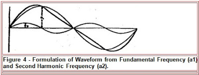
Some idea of the order of the harmonic can often be determined from the shape of the waveform. Figure 4 illustrates the formation of a composite waveform from a fundamental frequency and its second harmonic at one quarter of the fundamental Amplitude. Figure 5 illustrates similar formation from a fundamental frequency and its third harmonic, also a quarter of the fundamental amplitude. In Figure 5(b), the phase of the harmonic is shifted 180 degrees to that in Figure 5(a), and in Figure 5(c), the phase is shifted 90 degrees to that in (5a). The figures show that the composite wave forms can be quite different for different phase conditions making resolution sometimes tricky.


Some distorted waveforms directly indicate an out of adjustment or incorrect operating condition. The clipped waveform of Figure 6(a) shows the output of an amplifier driven to an overload or saturated condition. Figure 6(b) is clipped in one direction indicating an off-centre setting of an amplifier operating point. Figure 6(c) shows crossover distortion in a Class B amplifier.


Another method of testing, using sine waves, is to feed the monitored device input signal to the X plates input of the CRO and the device output signal to the Y plates input of the CRO. This plots the transfer characteristic of the device, that is, instantaneous output voltage as a function of instantaneous input voltage. X and Y gain is adjusted for equal vertical and horizontal scan. A perfect response is indicated by a diagonal line on the screen, or with phase shift, an ellipse or circle. Figure 10 shows various fault wave forms taken from one reference source. The different effects are explained in the diagram captions


The same connection can be used to measure phase shift between two sine wave signals of the same frequency such as measuring the phase shift between the output and input of an amplifier. Typical measurements are shown in Figure 8. A straight forward sloped diagonal line indicates no phase shift. A straight reverse sloped diagonal line indicates 180°. A circle indicates 90° and an elipse 45° or 135°.


If a dual trace CRO is available, the two signals can be displayed together, one on each vertical or Y trace with normal X sweep. In this case, it is simply a matter of scaling off the phase difference along the Y axis graticle.
Section B - Spectrum Analyser Waveforms
Over the years, the cathode ray oscilloscope (CRO) has been a universal instrument for examining analogue signals. Rapid advances in technology have led to a era of microcomputer controlled, digitally controlled test equipment, not the least of which is the modern spectrum analyser which enables greater precision analysis of analogue signals than is possible with the CRO. A spectrum analyser plots signal amplitude (or signal power) as a function of frequency compared to the CRO which plots signal amplitude as a function of time.
The spectrum analyser is not the type of equipment normally within the reach of the radio amateur and because of this, it was thought that it would be of interest to illustrate a few spectrum plots of well-known waveforms.
BASIC WAVEFORMS
Figure 1 shows the spectrum of a sine wave oscillator with fundamental at 1000 Hz and harmonics up to 20 kHz. The highest level harmonic at 7 kHz is 70 dB below the fundamental, representing a harmonic distortion of 0.03 percent. This is a very good oscillator which would not be matched by many laboratory instruments. It can also be seen that the noise floor is about 95 dB below the fundamental and this is also very good. The oscillator noise level might be even better than this as much of the noise is due to the spectrum analyser itself.
Figure 2 shows a 1000 Hz square wave. A perfect square wave generates odd harmonics to infinity with an amplitude 1/n relative to that of the fundamental or (20 log n) dB below the fundamental. ('n' is the order of harmonic). For n = 3, 5, 7 and 9 this calculates to -9.5, -14, -16.9 and -19.1 dB respectively, very close to the readings shown in Figure 2.


Figure 3 is the same square wave plotted out to 200 kHz and showing the apparently unlimited spread of harmonics. From this, it is easy to see why a low frequency square wave oscillator can be used as a marker generator over a wide frequency range.
Figure 4 shows a 1000 Hz triangular wave. A perfect triangular wave also generates odd harmonics to infinity, but each amplitude is (l/n) squared relative to the fundamental or (40 log n) dB below the fundamental. For n = 3, 5, 7, and 9, the calculation is -19, -28, -33.8, and -38.2 dB respectfully, again very close to the readings shown.


MODULATION
Figure 5 shows a 1 MHz carrier frequency, amplitude modulated by a frequency of 1 kHz to a modulation depth of 50 percent. For this case, the two side frequencies, 1 kHz either side of the carrier, are 12 dB below the carrier level, or a quarter of its amplitude. Other side frequencies at 2 kHz and 3 kHz, either side of the carrier, are the result of harmonics either in the original modulating tone or distortion caused by the modulation process. The 2 kHz side frequencies are about 30 dB below the 1 kHz side frequencies representing about three percent distortion in the system.
In Figure 6, the modulation level has been increased to 100 percent and the side frequencies, 1 kHz either side of the carrier, are now 6 dB below carrier level, or half its amplitude. The spectrum has been expanded to show many more harmonically related sideband components which now appear. Except for those close to the carrier, most of the components are more than 50 dB down and not of any great concern.


In Figure 7, the carrier is over-modulated and there is now a spread of sideband components about 30 dB down. If this were an amateur radio transmitter, other amateur stations in nearby suburbs would be complaining about sideband splatter.
Figure 8 Shows a 1 MHz carrier, frequency modulated by a 1 kHz tone with a deviation of 8.650 kHz, representing a modulation index of 8.650. It can be seen that there are many side frequencies all spaced by an amount equal to the modulating frequency (1 kHz). For this signal, a significant bandwidth of about 20 to 30 kHz is being utilised.


If we now examine Figure 9, which plots the amplitude of the carrier and side frequencies against the value of modulation index, we can see that there are a number of values of modulation index where the carrier level becomes zero. These are very convenient references to calibrate the amount of deviation. In Figure 8, the deviation has been set to produce the third carrier null at a modulation index of 8.650, so we know precisely that with our modulating frequency of 1000 Hz, our deviation is 8.650 x 1000 = 8850 Hz.


FREQUENCY RESPONSE
Another useful function of the spectrum analyser is to plot the frequency response of a four terminal device such as an amplifier or a filter. In this case, the analyser frequency sweep generator is fed to the input of the device and the output of the device is fed to the input of the analyser. Typical plots of a low pass filter and a bandpass filter are shown in Figures 10 and 11 respectively


Lenny Z Perez M
EES


Get news, entertainment and everything you care about at Live.com. Check it out!