This time in Basic Circuits, I would like to discuss bypass capacitors. This article will explain the function of a bypass capacitor, when its appropriate to use them, and what values you should consider using.
The Function
The definition of a bypass capacitor can be found in the dictionary of electronics.
Bypass capacitor: A capacitor employed to conduct an alternating current around a component or group of components. Often the AC is removed from an AC/DC mixture, the DC being free to pass through the bypassed component.
In practice, most digital circuits such as microcontroller circuits are designed as direct current (DC) circuits. It turns out that variations in the voltages of these circuits can cause problems. If the voltages swing too much, the circuit may operate incorrectly. For most practical purposes, a voltage that fluctuates is considered an AC component. The function of the bypass capacitor is to dampen the AC, or the noise. Another term used for the bypass capacitor is a filter cap.

In the chart, you can see the what happens to a noisy voltage when a by-pass capacitor is installed. Notice that the differences in voltage are pretty small (between 5 and 10 millivolts). This graph represents a small range of 4.95 volts to 5.05 volts. Random electrical noise causes the voltage to fluctuate, as you can see in graph. This is often called 'noise' or 'ripple'. The blue line, represents the voltage of a circuit that doesn't have a bypass. The pink line is a circuit that has a bypass. Ripple voltages are present in almost any DC circuit. You can see even with the bypass, the voltage does fluctuate, even though it is to a smaller degree. The key function of the bypass capacitor is to reduce the amount of ripple in a circuit. Too much ripple is bad, and can lead to failure of the circuit. Ripple is often random, but sometimes other components in the circuit can cause this noise to occur. For example, a relay or motor switching can often times cause a sudden fluctuation in the voltage. Much like disturbing the water level in a pond. The more current the other component uses, the bigger the ripple effect.
A fair question to ask is why does this small fluctuation matter? Gee, isn't the voltage close enough? The answer depends on the type of circuit you are designing. If you are just running a motor connected to a battery, or perhaps an LED, then chances are the ripple doesn't matter much to you. However, if you are using digital logic gates, things get slightly more complex, and this ripple can cause problems in the circuit.
Lets consider for just a moment what the effect of the ripple voltage is. Basic electrical theory tells us that a voltage is a difference in potential. It tells us that a current will flow across this difference in potential. We know that the larger the voltage, the larger the current. We also know the direction of the voltage determines the direction of the current.
| Consider the graphs. The top graph shows a pair of ripple voltages that I enlarged to make them easier to see. Just like the previous graph, the blue line represents the circuit without the bypass cap, and the other line is with the bypass cap. By looking along the bottom axis of the graph, you can see that starting at point 2 that the voltage is increasing. By looking in the Ripple Current chart, point 2 shows that the current is a relatively large magnitude in one direction. In contrast, point 5 shows the voltage and current going the other direction. Notice the difference between the values with and without the bypass cap. By dampening the ripple voltage, the bypass cap also dampens the ripple current. I would like to point out that the Ripple Voltage chart and the Ripple Current charts clearly show an alternating current. You can see how the voltage swings, and how the current changes directions. Even though this is is a DC circuit, the ripple is causing an AC component. The bypass capacitor is helping to reduce this AC component. The ripple current acts like an eddie or backflow in the circuit. As the fluctuating voltages and currents propogate through the circuit, differences in voltages and currents can occur that cause the circuit to fail. For example, assume that a AND gate is holding its state because the semiconductors that make up the gate are in a stable state. Transistors work by currents flowing one direction through the gate. If the current stops flowing, the transistor shuts down. If a ripple current comes through where the current momentarily flows the wrong direction, the gate will shutdown, and you will see a change it its output. This can cause a cascading failure, because one gate may be connected to many other gates. |


To summarize, the bypass capacitor is used to dampen the AC component of your DC circuits. By installing bypass capacitors, your DC circuit will not be as susceptable to ripple currents and voltages.
Using Bypass capacitors
Many schematics that you find published in magazines and books leave the bypass capacitors out. They assume you know to put them in. Other times you will find a little row of capacitors (caps) stuck off in the corner of the schematic with no apparent function. These are usually the bypass (or filter) caps. If you pickup almost any digital circuit, you will find a bypass capacitor on it.

The most simple incarnation of the bypass capacitor is a cap connected directly to the power source and to ground, as shown in the diagram to the left. This simple connection will allow the AC component of VCC to pass through to ground. The cap acts like a reserve of current. The charged capacitor helps to fill in any 'dips' in the voltage VCC by releasing its charge when the voltage drops. The size of the capacitor determines how big of a 'dip' it can fill. The larger the capacitor, the larger the 'dip' it can handle. A common size to use is a .1uF capacitor. You will also see .01uF as a common value. The precise value of a bypass cap isn't very important.
So, how many bypass capacitors do you really need? A good rule of thumb I like to use is each IC on my board gets its own bypass capacitor. In fact, I try to place the bypass cap so it is directly connected to the Vcc and Gnd pins. This is probably overkill, but it has always served me well in the past, so I will recommend it to you. It turns out you can even by DIP sockets that have the bypass caps built in. I suppose once you reach more than a few capacitors per square inch, you might be able to let up a bit!
Another great place for a bypass cap is on power connectors. Anytime you have a power line heading off to another board or long wire, I would recommend putting in a bypass cap. Any long length of wire is going to act like a little antenna. It will pick up electrical noise from any magnetic field. I always put a bypass cap on both ends of such lengths of wire.
The type of capacitor you use can be important. I would recommend you use a monolithic ceramic capacitor. They are small, cheap, and readily available. I usually use a .1uF 50Volt +-20% with .1" or .2" spacing. Again, .01uF is also acceptable. I would avoid larger voltage capacitors as they are physically too large. Electrolytic capacitors are not well suited to the role of bypass capacitors as they typically have larger capacitance values and don't respond as well to high frequency changes.
| The frequency of the ripple can have a role in choosing the capacitor value. Rule of thumb is the higher the frequency, the smaller the bypass capacitor you need. If you have very high frequency components in your circuit, you might consider a pair of capacitors in parallel. One with a large value, one with a small value. If you have very complex ripple, you may need to add several bypass capacitors. Each cap is targeting a slightly different frequency. You may even need to add a larger electrolytic cap in case the amplitude of the lower frequencys is too great. For example, the circuit on the right is using three different capacitor values in parallel. Each will respond better to different frequencies. The 4.7uF cap (C4) is used to catch larger voltage dips which are at relatively low frequencies. The cap C2 should be able to handle the midrange frequencies, and C3 will handle the higher frequencies. The frequency response of the capacitors is determined by their internal resistance and inductance.
|

Summary
Bypass capacitors help filter the electrical noise out of your circuits. They do this by removing the alternating currents caused by ripple voltage. Most digital circuits have at least a couple of bypass capacitors. A good rule of thumb is to add one bypass capacitor for every integrated circuit on your board. A good default value for a bypass cap is 0.1uF. Higher frequencies require lower valued capacitors.
Coupling (electronics)
In electronics and telecommunication, coupling is the desirable or undesirable transfer of energy from one medium, such as a metallic wire or an optical fiber, to another medium, including fortuitous transfer.
Coupling is also the transfer of power from one circuit segment to another, e.g., an alternating voltage may be transferred to a segment at a different direct voltage by use of a capacitor or transformer; power may be efficiently transferred to a segment with different impedance by use of a transformer.
Types of coupling
*Electromagnetic coupling:inductive coupling, most commonly transformer coupling, also called magnetic coupling
*capacitive coupling, capacitor coupling, also called electrostatic coupling
*RF coupling
*electromagnetic interference (EMI), sometimes called radio frequency interference (RFI), is unwanted coupling. Electromagnetic compatibility (EMC) requires techniques to avoid such unwanted coupling, such as electromagnetic shielding.
*wireless energy transfer
*Other kinds of energy coupling:acoustic coupling with an acoustic coupler, evanescent wave coupling
Capacitive coupling
In electronics, capacitive coupling is the transfer of energy within an electrical network by means of the capacitance between circuit nodes. This coupling can have an intentional or accidental effect. Capacitive coupling is typically achieved by placing a capacitor in series with the signal to be coupled.
Use in analog circuits
In analog circuits, a coupling capacitor is used to connect two circuits such that only the AC signal from the first circuit can pass through to the next while DC is blocked. This technique helps to isolate the DC bias settings of the two coupled circuits. Capacitive coupling is also known as AC coupling and the capacitor used for the purpose is known as a coupling or DC blocking capacitor. Capacitive coupling has the disadvantage of degrading the low frequency performance of a system containing capacitively coupled units. Each coupling capacitor along with the input electrical impedance of the next stage forms a high-pass filter and each successive filter results in a cumulative filter with a -3dB frequency that may be higher than each individual filter. So for adequate low frequency response the capacitors used must have high capacitance ratings. They should be high enough that the reactance of each is at least ten times the input impedance of each stage, at the lowest frequency of interest. This disadvantage of capacitively coupling DC biased, transistor amplifier circuits is largely minimized in directly coupled designs.
Use in digital circuits
AC coupling is also widely used in digital circuits to transmit digital signal with a zero DC component, known as DC-balanced signals. DC-balanced waveforms are useful in communications systems, since they can be used over AC-coupled electrical connections to avoid voltage imbalance problems and charge accumulation between connected systems or components.
For this reason, most modern line codes are designed to produce DC-balanced waveforms. The most common classes of DC-balanced line codes are constant-weight codes and paired-disparity codes.
Gimmick
A "gimmick" is a very simple kind of capacitive coupling: a piece of wire that is placed in proximity to another one, providing a capacitive coupling between two nodes of a few picofarads in value. Sometimes the wires are twisted together for physical stability.[1][2]
Parasitic capacitive coupling
Capacitive coupling is often unintended, such as the capacitance between two wires or PCB traces that are next to each other. Often one signal can capacitively couple with another and cause what appears to be noise. To reduce coupling, wires or traces are often separated as much as possible, or ground lines or ground planes are run in between signals that might affect each other. Breadboards are particularly prone to these issues due to the long pieces of metal that line every row creating a several-picofarad capacitor between lines. To prototype high-frequency (10s of MHz) or high-gain analog circuits, often the circuits are built over a ground plane so that the signals couple to ground more than to each other. If a high-gain amplifier's output capacitively couples to its input it often becomes an oscillator.
BJT NPN

Coupling Capacitor (C1)
The cutoff frequency due to C1 can be calculated by
fL1= 1/(2∏(R1+Ri)*C1)
Where
Ri=R2 R3 ßre
Coupling Capacitor (C2)
The cutoff frequency due to C2 can be calculated with
fL2= 1/(2∏(Ro+R6)*C2)
Where
Ro=R2 r0

JFET
Coupling Capacitor (C1)
The cutoff frequency due to C1 can be calculated with
FL1= 1/(2∏(R1+Ri)*C1)
Where
Ri=Rg
Coupling Capacitor (C2)
The cutoff frequency due to C1 can be calculated with
FL1= 1/(2∏(Ro+R5)*C2)
Where
R0= R3 rd
The cascode amplifier
While the C-B (common-base) amplifier is known for wider bandwidth than the C-E (common-emitter) configuration, the low input impedance (10s of Ω) of C-B is a limitation for many applications. The solution is to precede the C-B stage by a low gain C-E stage which has moderately high input impedance (kΩs). See Figure below. The stages are in a cascode configuration, stacked in series, as opposed to cascaded for a standard amplifier chain. See "Capacitor coupled three stage common-emitter amplifier" Capacitor coupled for a cascade example. The cascode amplifier configuration has both wide bandwidth and a moderately high input impedance.

The cascode amplifier is combined common-emitter and common-base. This is an AC circuit equivalent with batteries and capacitors replaced by short circuits.
The key to understanding the wide bandwidth of the cascode configuration is the Miller effect Miller effect. It is the multiplication of the bandwidth robbing collector-base capacitance by beta. This C-B capacitance is smaller than the E-B capacitance. Thus, one would think that the C-B capacitance would have little effect. However, in the C-E configuration, the collector output signal is out of phase with the input at the base. The collector signal capacitively coupled back opposes the base signal. Moreover, the collector feedback is beta times larger than the base signal. Thus, the small C-B capacitance appears beta times larger than its actual value. This capacitive gain reducing feedback increases with frequency, reducing the high frequency response of a C-E amplifier.
A common-base configuration is not subject to the Miller effect because the grounded base shields the collector signal from being fed back to the emitter input. Thus, a C-B amplifier has better high frequency response. To have a moderately high input impedance, the C-E stage is still desirable. The key is to reduce the gain (to about 1) of the C-E stage to reduce the Miller effect C-B feedback to 1•CCB. The total C-B feedback is the Miller capacitance 1•CCB plus the actual capacitance CCB for a total of 2•CCB. This is a considerable reduction from β•CCB.
The way to reduce the common-emitter gain is to reduce the load resistance. The gain of a C-E amplifier is approximately RC/RE. The internal emitter resistance REE at 1mA emitter current is 26Ω. For details on the 26Ω, see "Derivation of REE", see REE. The collector load RC is the resistance of the emitter of the C-B stage loading the C-E stage, 26Ω again. CE gain amplifier gain is approximately RC/RE=26/26=1. We now have a moderately high input impedance C-E stage without suffering the Miller effect, but no dB voltage gain. The C-B stage provides a high voltage gain. Thus, the cascode has moderately high input impedance of the CE, good gain, and good bandwidth of the C-B.
.
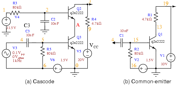
SPICE: Cascode and common-emitter for comparison.
The SPICE version of both a cascode amplifier, and for comparison, a common-emitter amplifier is shown in Figure above. The netlist is in Table below. The AC source V3 drives both amplifiers via node 4. The bias resistors for this circuit are calculated in an example problem cascode.

SPICE waveforms. Note that Input is multiplied by 10 for visibility.
SPICE netlist for printing AC input and output voltages
Lenny Z. Perez M
EES
Referencias:
http://www.seattlerobotics.org/Encoder/jun97/basics.html
http://en.wikipedia.org/wiki/Coupling_(electronics)
http://macao.communications.museum/images/exhibits/small/2_16_6_1_eng.png
http://macao.communications.museum/images/exhibits/small/2_16_3_1_eng.png
Explore the seven wonders of the world Learn more!
Explore the seven wonders of the world Learn more!
No hay comentarios:
Publicar un comentario